12. Q-switches
A Q-switch is a mechanism that concentrates the varying intensity emission pulses of a laser into a short pulse of intense energy. Q-switches employ an optical medium that blocks light until electrically or mechanically released.
Much as I hate Grok, here is a very informative page I discovered in 2026, long after I created this:
https://grokipedia.com/page/Q-switching
A good explanation of Q-switching is given here: http://www.rp-photonics.com/q_switching.html
[L3]: Laser-Induced Breakdown Spectroscopy, reveals the need for Q-switching in LIBS systems:
'If the laser is pumped by a flashlamp, pulse widths in the range of 100µs to 1ms are typical. In many cases, the laser emission is not uniform, but consists of many microsecond duration spikes called relaxation oscillations whose amplitudes and spacing are not uniform. The presence of these spikes in the laser pulse causes heating and cooling of the target surface and is not suitable for producing a uniform plasma plume'.
The LHC project's NLO-based UV conversion scheme needs the extra power afforded by Q-switching and [L3] indicates it is essential for LIBS anyway, so I needed to Q-switch the lasers.
Q-SWITCH MECHANISMS
In the distant past, mechanical shutters were used that typically consisted of a rotating mirror or prism, the down side to these being poor timing repeatability due to the variation of the high speed motor, and eventual failure of the bearings.
[O3], Solid-State Lasers - A Graduate Text:
'A key discovery made by R.W. Hellwarth in 1961 was a method called Q-switching for concentrating the output from the ruby laser into a single pulse. The Q-switch is an optical shutter which prevents laser action during the flashlamp pulse, therefore the population inversion can reach large values. If the shutter is suddenly opened, stored energy will be released in a time characterized by a few round trips between the resonator mirrors. With Q-switching, several round trips are required for radiation to build up. Given the length of the resonator and available gain of these early systems, the pulses were on the order of 10 to 20ns.
KERR CELL / SPINNING MIRROR / SPINNING PRISM
Hellwarth initially proposed a Kerr cell, a device which rotates the plane of polarization when voltage is applied. This Q-switch, which consisted of a cell filled with nitrobenzene, required very high voltages for Q-switching; it was soon replaced by spinning one of the resonator mirrors. A further refinement was the insertion of a spinning prism between the fixed mirrors of the resonator.
Q-SWITCH (10-20ns)
CAVITY-DUMPING FAST Q-SWITCH [(1-10ns) my guess]
The next step toward shorter pulses was a technique called cavity dumping, whereby the radiation in the resonator, as it reached its peak, was quickly dumped by a fast Q-switch. Pulses with a duration on the order of one round trip (a few nanoseconds) in the resonator could be generated with this method.
MODE-LOCKING (20-100ps)
In 1965, a technique termed 'mode-locking' was invented. Mode-locking is a technique whereby passive loss modulation, with a fast response saturable absorber, or by active loss of frequency modulation, a fixed relationship among the phases of the longitudinal modes is enforced. With either passive or active mode-locking, pulses much shorter than a resonator round trip time can be generated; typically, pulses are on the order of 20 to 100ps.'
POCKELS CELL
A Pockels cell is the modern day equivalent of a Kerr cell, and slightly easier to drive. It too consists of a crystal that alters the angle of polarisation of light passing through it when a voltage is placed across it. The higher the voltage, the greater the angle: half wave rotation requires double the voltage needed for quarter wave rotation. Typically the cell is placed in the laser resonator followed by a quarter waveplate. When the cell rotation matches that of the waveplate the light passes through, otherwise it is blocked. A typical voltage for a pockels cell to match a quarter waveplate
is something in the order of a 3.4kV. Dc voltage stresses the cell so short pulse are used instead.
[N17], Pockels Cell Primer, provides a good introduction to these devices. A brief summary is below:
http://www.leysop.com/app_note_1.htm
'First described in 1906 by F. Pockels, the linear electro-optic effect occurs in crystals which lack a centre of symmetry and is observed as a change in refractive index produced by an applied electric field. The change is small, but is sufficient to alter the spatial phase condition of light.
To make use of this effect, light must propagate through the crystal normal to a direction in which the refractive index change can be produced. Two terminal Pockels cell for Q-switching. If the incident polarisation direction is at 45° to the principle refractive index values, then the light will exit the crystal as two orthogonal components with a phase difference between the ordinary and the extra-ordinary ray which is linearly proportional to the applied electric field. These components combine in space to form generally elliptical polarisation states (linear and circular polarisation being special forms of elliptical polarisation).
The Pockels cell designer must choose an appropriate material which produces a large induced birefringence and then maximize its effect by a sensible choice of crystal cut, light path and applied electric field directions. When the electric field is applied along the light path then the modulator is referred to as longitudinal and if the field is across the light path, then the modulator is transverse.
The most frequently used materials for longitudinal mode Pockels cells are KDP and more commonly, the deuterated form KD*P. This has a modest half wave voltage (the voltage which must be applied to produce a pi radian phase shift, equal to a polarisation rotation of 90°) of around 6kV at 1064nm and has extremely high resistance to laser damage as well as being available in excellent quality crystals of large sizes. For these reasons, all our longitudinal mode Pockels cells are manufactured from >95% deuterated KD*P.'
Inrad pockels cell part numbers
Several manufacturers exist, but the one that most often crops up in old papers or on eBay is Inrad, notably in the form of their legacy numbered nnn-nnn series and their modern equivalent PxC-xxn series.
Google AI:
APERTURE
a.Mechanical Aperture (MA): The physical diameter of the hole or crystal face.
b.Clear Aperture (CA): The specified central area of that optic (usually 80% to 90% of the MA).
The outer 10% to 20% perimeter of the optic is excluded from the CA because of physical limitations
such as edge distortions, field uniformity and mounting scratches.
In a Pockels cell electric field lines degrade or bend near the metal ring electrodes at the outer
edges. If a manufacturer states a cell has a 10mm CA the physical crystal inside is actually larger
e.g.12mm, ensuring the laser beam has an unobstructed path across its entire 10mm.
c.Usable Aperture (UA): Even if a crystal has a 10mm CA it will not safely pass a 10mm diameter HE
Gaussian or top-hat beam through it because wings of the beam will clip the edges of the clear
aperture. This causes diffraction rings (which distort the beam profile) and can instantly burn the
housing or destroy the crystal's edge coatings.
As a rule of thumb, UA (beam diameter) should be no more than 60% to 70% of the listed clear aperture.
AR COATINGS
Standard catalog cells were coated for the primary 1064nm Nd:YAG laser line.
Custom variants changed the thin-film window coatings for other wavelengths:
Visible Spectrum: 694nm (Ruby lasers) or 532nm (Frequency-doubled YAG).
UV Spectrum: 266nm or 355nm for UV harmonic generation.
Broadband/Tunable: specially shifted coatings for Ti:Sapphire lasers (700-900nm) or dye lasers.
DEUTERATION
a.lowers operating voltage: Deuteration doubles the material's electro-optic coefficient, halving the
high voltage required to switch the laser beam.
b.minimises absorption: replacing regular hydrogen with heavier deuterium eliminates parasitic light
absorption within key near-infrared laser wavelengths.
c.eliminates thermal lensing: reducing optical absorption prevents localized internal heating, which
keeps the passing laser beam perfectly focused and free of distortion.
d.increases damage threshold: minimising internal thermal hotspots allows the crystal to withstand
significantly higher peak laser energy without cracking or sustaining damage.
e.Suppresses Raman Scattering: altering the internal vibrational frequencies of the crystal lattice
blocks parasitic scattering that can divert laser energy and cause structural failure.
Standard KD*P crystals are typically ~95% deuterated. A specialised high-deuteration >99% variant dramatically lowers optical absorption and prevents the crystal from overheating.
CONNECTORS
BNC or SMA inputs (common on the 212 series for low-voltage, fast pulse-picking applications).
HN or SHV connectors (for safe, shielded high-voltage handling up to 10kV).
DRIVING VOLTAGE
Standard KD*P Q-switches require a quarter-wave voltage (Vπ/2) to act as a shutter. At 1064nm (Nd:YAG), this voltage is typically around 3.2kV to 3.6kV. Because the required voltage drops linearly with wavelength λ, an Inrad cell operating at 755nm only requires roughly 2.3kV to 2.5kV to successfully
Q-switch the cavity.
Inrad Legacy part numbers
SERIES
202 Series (standard fluid-filled / dry longitudinal KD*P)
This was Inrad's most widely distributed series for standard Q-switching, typically featuring cylindrical housings with windows enclosing a deuterated potassium dihydrogen phosphate (KD*P) crystal.
202-040: often utilized in small-aperture scientific dye or Nd:YAG lasers
202-050: 5mm clear aperture variant
202-080: 8mm clear aperture, common in military/aerospace rangefinders
202-090: 9mm clear aperture, a legacy predecessor to the modern PKC21-SG09
202-100: 10mm clear aperture, a variant
202-150: 15mm clear aperture, a variant for higher energy pulse extraction
202-160: 16mm clear aperture, heavy-duty industrial laser variant
202-909: 9mm clear aperture, specialized >99% high-deuteration build
212 Series (impedance matched / fast rise time / dual crystal
The 212 series was engineered for applications requiring faster optical rise times, higher repetition rates, or lower driving voltages, often utilizing a dual-crystal design where crystals are optically in series but electrically in parallel.
212-040: small aperture, fast-switching variant
212-050: highly common in legacy regenerative amplifiers and pulse-pickers
212-080: balanced impedance 8mm cell
212-090: 9mm fast-rise Q-switch, often matching early 50Ω drivers
212-100: 10mm version for amplified laser lines
250 & 260 Series (large aperture & high power)
These numbers were assigned to specialised, larger housings built for high-energy Nd:Glass or ruby laser amplification systems.
252-150: 15mm specialty aperture housing
252-200: 20mm large aperture variant
262-250: 25mm extra-large aperture, predecessor to the modern PKC21-SG25
nnn-400: configured for Ruby lasers (694nm) or frequency-doubled wavelengths (532nm)
nnn-700: custom builds
nnn-900: broad-band or specific Alexandrite or Ti:Sapphire tuning configurations (~700-900nm)
Inrad modern part numbers, Google AI:
Modern part numbers are divided into three chemistries:
Series Chemistry λ range Peak damage threshold **CW Average damage threshold
PKC KD*P 250nm - 1.32μm, >800MW/cm²
PBC BBO 220nm - 2.1μm, >500MW/cm²
PLC LiNbO₃ 1.064μm - 4.0μm, >300 MW/cm² >100 W/cm²
**Unlike KD*P and BBO, which are overwhelmingly used for short, ultra-intense nanosecond pulses, Lithium Niobate's physical properties mean it is also frequently evaluated for continuous-wave (CW) applications or high-duty-cycle modulation.
INDEX-MATCHING
In legacy 202 cells, index-matching fluid (perfluorocarbon, e.g. FC-43) was needed to stop reflections between the window and the crystal. Modern cells apply a Sol-Gel AR coating directly onto the crystal face inside a dry, hermetically sealed housing. This eliminates fluid degradation and drastically raises the laser damage threshold.
[N26] below lists Inrad modern series standard parts and available variants circa 2014.
Other Inrad part numbers
The 530 designation defines the physical metal-and-perspex body frame, the clear-view fluid cavity configuration, and the 2mm banana pin layout. Inrad engineered the 530 architecture as a 'universal modular cell'. Depending on how a laboratory ordered it, Inrad would assemble this exact same 530 mechanical body for both pockels cells and harmonic crystals.
530-010: a specialized small-aperture version featuring a 5mm clear aperture, typically optimized for low-profile dye laser inputs to handle tight focal points without internal window edge clipping.
530-020: a 15mm long crystal variant designed for mid-power setups, acting as an early alternative to internal cavity Q-switches.
530-080: the definitive baseline catalog part number. This is the exact mechanical twin to your cell, utilizing an 8mm to 10mm aperture.
530-081: standard 10mm x 10mm crystal cell configuration housing small-aperture KDP/KD*P crystals (often matched with size 5-14B crystal cuts). An upgraded iteration of the -080. It added enhanced, fine-threaded alignment adjustments on the window housings to better suppress internal parasitic feedback reflections.
530-090: a high-power deep variant engineered with an extended fluid reservoir volume to help cushion acoustic shocks and allow faster thermal dissipation under repetitive pulses.
531 / 541 Series: Mid-sized housings holding 13.5mm x 13.5mm x 15mm crystals.
532 / 542 Series: Extended-length crystal cells housing longer 13.5mm x 13.5mm x 30mm KDP crystals for higher conversion efficiency.
562-126: a specialized 6.75mm x 13.5mm x 30mm crystal variant optimized for automated tuning systems.
563-1117: a larger 13.5mm x 18.5mm x 30mm configuration, standard in legacy automated systems like the Inrad Autotracker II.5-050: Often paired alongside these series as a commercial tripler or high-order harmonic generator.
N- Series
I have a N-530A KD*P HD 1 AR 1.06 FC43 on an XY mount with basic (non-vernier) hand adjustment knobs. The body is clear perspex or similar with what looks like thick aluminium end plates.I measured 6.2pF across its pins which are the old generation pockels cell 2mm banana type.
Prefix N- = Non-Standard build.
Suffix -A = crystal cut orientation or phase-matching type (Type I vs. Type II phase matching)
HD 1 = High Deuteration >99%.
ROTARY SHUTTER Q-SWITCH
I found a paper describing an experiment using a mechanical optical shutter as an active Q-switch:
[O14], Performance of a Diode-Pumped Laser Repetitively Q-Switched with a Mechanical Shutter. This article used a relatively low speed, standard optical shutter to Q-switch a relatively modern diode pumped laser.
A light bulb lit in my head: conventional non-passive Q-switches are rather bulky and this is a problem with the MK580 which is constructed on its own aluminium frame complete with IC and OC already aligned and operational. There is very little room to fit anything between them, but it might just be possible to slip in the disc from an optical chopper.
This in turn leads to another possibility - I had already planned to use an optical chopper to block Bremsstrahlung radiation to the spectrometer, and the laser firing needs to be synchronised to it.
I had acquired two MK580s and I was considering expanding the resonator on one of them to accommodate a Pockels cell and the necessary waveplate and aperture. I knew the length of the resonator is critical to operation but I was willing to experiment. The second laser for frequency summing to DUV would be DIY anyway, so not a problem. I was going initiate their firing from the optical chopper disc, but I was reluctant to disturb the mirrors on a perfectly functional Nd:YAG laser.
What if I could use the same chopper to block Bremsstrahlung radiation, as well as Q-switch one MK580 and the experimental second laser, thus synchronising them, based upon the experiments in [O14]?
However:
Conventional mechanical Q-switches consist of a rotating mirror or prism. The DIY laser somewhat poorly described in [O36] 'Solid-State lasers for the Laser Enthusiast', utilises a spinning mirror producing an 8ns pulse. The original Hughes ruby laser rangefinder used a spinning prism:

The mechanical shutter in [O14] makes no mention of any mirrored surface, and a Pockels cell isn't exactly reflective when it is off, either. If there is no mirror to bounce back off, why does the beam get amplified? MORE RESEARCH NEEDED
Paper [O60] compares Mech chopper vs AO vs EO Q-Switch mechanisms for a 1550nm FO Er:Yb laser. It concludes EO pockels produces the highest power followed by AO Pockels, followed by mechanical, which IMO is hardly surprising: the OE most closely tracks the pulse and therefore has the lowest losses.
However they still managed to get 15.5kW out of it with the chopper, and they used the same chopper as mine: Scitec 300CD, and their measurements were taken with the same chopper discs I have see
[Spectral Gating], so I can repeat their same experiments with my chopper and the M580KK Nd:YAG.
ACOUSTO-OPTIC MODULATORS
Acousto-optic modulators typically switch Pockels cells at the µs rate rather than the ns rate of Electro-optic q-switches in order to modulate signals onto an existing laser output, but the principle is largely the same.
At first I discounted AO due to the low speed, but RP-Photonics Encyclopedia [212p01] makes an interesting point: https://www.rp-photonics.com/q_switching.html
'...the switching time of the modulator does not need to be comparable to the pulse duration – it can be much longer than that, since it takes many resonator round trips for an intense pulse to be formed. If it is too long, however, this may lead to double pulses or to certain instabilities.'
This is interesting for two reasons: my LIBS system is typically a single pulse system, although papers have shown emission intensifies with multiple pulses, up to 7, at the expense of shorter flashlamp life.
The MK367 passive Q-switched Nd:YAG builds up the energy for its q-switch pulse from multiple passes through its resonator until the output coupler is saturated and releases it as a large pulse.
I found a Lysop 5000 EO modulator on eBay UK for £250 and bought it thinking I could use it to explore Pockels cell operation at lower frequencies (fastest rate is 14µs) as part of my Pockels cell driver design research, also contemplating using it as a pulsed voltage source from which I could gate shorter, ns Q-switch pulse. It's supposed to produce a 5kV signal which I assume means ±2k5V, but at present it's only producing ±1k7V, so awaiting repair. I could find no manual let alone a schematic, so it will have to be a reverse engineering job that I've been putting off due to the high voltages involved.
However given the low pulse rate of a LIBS system, it may be possible to get away with using the Lysop 5000 as the pockels driver itself. AGAIN, MORE RESEARCH NEEDED
There is yet another option I have not seen mentioned elsewhere, doubtless because laser system design is about meeting a customer's needs rather than bodging an existing design to work differently:
I have no room in the MK580 cavity for anything but a rotating disc, but why can't I just place a pockels cell after its OC?
I had not yet acquired the Lysop when I decided the following plan of action:
Knowing my luck with far-fetched ideas, I realised the chance of a triple mechanical shutter synchronisation system working was pretty low. I would try it, but surely the ideal setup would be to use pockels cells throughout. I would clearly have to design my own resonators to accommodate them, and I made preparations for this likely conclusion. Given the absence of affordable pockels drivers on eBay and the expense of OEM assemblies, the next step was to determine the feasibility of building my own.
POCKELS CELL DRIVERS
Pockels cells are controlled using short pulses of several kilovolts having very fast rising or falling edges. [N16]: FastPulse guide to pockels cell drivers etc., describes several ways of driving them.
KDP / D*KDP pockels types are prone to ringing [N5]: Inrad PBC BBO pockels cells et al, which becomes evident the longer the cell is biased - read into this frequency of pulses - but this should not affect me as LIBS will not require many pulses. This also applies to the harmonic generator crystals.
Historical pockels cell drivers
In the past, Pockels cells and older Kerr cells were driven by electronic tubes such as Krytrons,
trigger tubes, triggered spark gaps, or hydrogen thyratrons particularly for high voltage gas lasers but these produce electrically noisy EMI, have a certain amount of inter-pulse hysteresis, usually involve custom inductor-based drive circuitry and are expensive. Furthermore hydrogen depletes over use and because of this there is no way of guaranteeing a hydrogen thyratron on eBay still works.
Here is a great website describing these older devices: http://www.electricstuff.co.uk/pulse.html
Here is a website with krytron specifications: http://www.siliconinvestigations.com/KRYT/Krytron.htm
UNCONVENTIONAL POCKELS CELL DRIVERS
[O34] A Simple Technique for Electro-Optic Q-Switching Using a Planar Photodiode, describes a particularly neat Pockels cell driver where a FEK-09 Tr300ps vacuum planar photodiode (VPD) is placed across the cell with its cathode to the +3.2kV quarter wave supply via 1.5MΩ, discharging the voltage when irradiated by light from the (Nd:YAG) laser cavity via a Glan prism. The VPD has low capacitance permitting discharge in <2ns, and a Q-pulse in the order of 20ns wide. Downsides are it consumes 1/3 of laser optical power, and it's impossible to find a FEK-09 VPD, or even a spec sheet; the nearest to this is in [O34]: 'Trise 300ps, Si photocathode, spectral sensitivity 0.1mA/W at 1.06µm, operating 2kV)',
'This photodiode has a linear-current response of as much as 18A and a sensitive area of 12.6cm²'.
I find it bizarre that few if any papers show photos of the instruments and equipment they blithely quote as if it will exist forever. I'd like to repeat the experiment and I haven't given up on the FEK-09 yet. As far as I can tell it was made in Russia, and there seems to be others in the series: FEK-19, FEK-22 and one 2015 paper is almost akin to the Rosetta Stone [G25] because it says 'With allowance for the required spectral sensitivity range, PGS-19, SPU-22, or FÉK-29 were used for photodetector 11.' [Multi-Wavelength Metal Vapor Laser Systems for Solving Applied Problems of Atmospheric Spectroscopy, A.Soldatov11, S.Mirza1, Y.Polunin1, A.Shumeiko1, I.Kostadinov2, National Research Tomsk State
University, Russia] implying there are several different manufacturers. The closest I've found is a site that confusingly lists a brief spec for the FEK-22-SPU-M from Russia's State Register, whatever that is,
with the entry dated 1979:
https://all--pribors-ru.translate.goog/opisanie/6989-79-fek-22-spu-m-65074?_x_tr_sl=ru&_x_tr_tl=en&_x_tr_hl=en&_x_tr_pto=sc
MORE DIGGING REQUIRED
The paper suggests it has the potential to synchronise different lasers: 'In an experiment to synchronize the laser with another laser, a part of the radiation from a laboratory built nitrogen laser was directed to the photodiode.', although I'm puzzled how you achieve this with differing lasing media having, I assume, differing Q-switch peak times.
They say they ran it for 3 months without issue but surely the Pockels cell has a dc voltage across it until the vacuum PT in parallel with it ionises and discharges its capacitance? Constant voltage is a recognised cause of shortened pockels cell life. Can the PT be placed in series with the Pockels cell?
MODERN POCKELS CELL DRIVERS
German manufacturer Behlke produces a range of encapsulated logic-level driven MOSFET arrays capable of switching several kilovolts at nanosecond speeds but they are prohibitively expensive. They do sell fully functional seconds at up to 50% off, but their cheapest part the HTS 50 which is capable of switching up 5kV at 30A with an internally fixed 100ns pulse width, was $198 (now no stock) and although they have a US presence, these special offers are only available from their German factory, slapping on a 19% tax to private sales. Otherwise a fantastically exotic device to experiment with:
[D26] Behlke HTS series general info, [D27] Behlke HTS 50 datasheet, website: http://www.behlke.com
A common low cost electronic approach employs a long string of transistors that rapidly switch the high voltage across the pockels cell when their breakdown voltage is exceeded as a result of the bottom transistor being switched on. This is known as running the transistors in avalanche mode.
An alternative design based on the same principle employs a Marx driver consisting of a string of transistors that switch in relatively low isolated voltages (typically 900V) in series, derived from capacitors on the common supply: http://en.wikipedia.org/wiki/Marx_generator
The disadvantage of both of these approaches is the breakdown voltage is unpredictable and by its nature, manufacturers naturally advise against operation in this region. Often pockels Q-switch designers using this approach mount the transistors in sockets and ship them with spares should the inevitable arise. I know, because I bought an ancient Inrad 2-015 driver out of curiosity and looked inside (it uses 2N4401s, see 'Others' transistor list in References: Avalanche Transistors section 7).
Going against the flow, Zetex Semiconductors produces transistors designed specifically to avalanche: ZTX413, ZTX415, ZTX417 and surface mount counterparts FMMT413, FMMT415, FMMT417, but they are relatively slow (1ns edges) and expensive ($10) in comparison to old mesa/epitaxial NPNs, unless bought in Asia, where there is also a large risk of counterfeit devices.
There are several articles on the web about avalanche drivers and many ordinary transistors have been investigated for suitability. Refer to References: Avalanche Transistors section 7 for a list of many of these papers and the transistors they used, and my test results.
Vbkdn = measured breakdown voltage
TrAvOC = open circuit avalanche rise time (TBD)
TfAvOC = open circuit avalanche fall time (TBD)
My final shortlist of transistors I tested for breakdown voltage (* = exceptional Vav):
Type Pol Freq Vce Vcb Vbkdn Icdc P Ppk Pkg TrAvOC TfAvOC COMMENTS
BF392 NPN 50MHz 250V=250V *416V 0.50A 0.63W 1.50W E-line I have 100
2N5551 NPN 100MHz 160V 180V *384V 0.30A 0.63W TO-92 I have 100
MMBT5551 NPN 100MHz 160V 180V *390V 0.60A 0.35W SOT23 I have 100
The generally favoured choice is a string of 2N5551 transistors. Following my evaluation, I decided it would be better to use SMD components to cut down inductance and capacitance and selected SOT-23
MMBT5551 NPN transistors instead.
This 1993 paper describes a Marx generator using TO-92 2N5551 transistors:
[A10], A Transistorised Marx Bank Circuit Providing Sub-nanosecond HV Pulses. However I set about building my own avalanche pockels cell driver based upon the design presented in what appeared to be an earlier 1990 version of it: [A6], A Fast Cavity Dumper for a Picosecond Glass Laser.
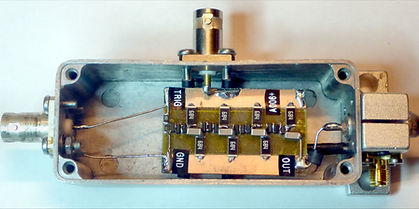
CONSTRUCTION
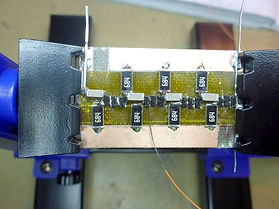
I decided to build the circuit on an off-cut of bare copper clad pcb which would have the +900V supply on one side and 0V on the other and a strip of missing copper in the middle.
To stand any chance of soldering SMD components within a tightly-dimensioned assembly, I decided to hold them in place before soldering. I could have used SMD adhesive compound but I wanted to be able to move and re-lay the components as I worked, so instead I used double-sided kapton tape which is readily available on eBay China. kapton tape withstands high voltages and temperatures and is available in several widths, although fewer in the double-sided version.
Laying out the components for one stage of the Marx generator on the ESD lab bench, I bore in mind
[E36], IPC-2221A Pcb Layout Standard, describing the minimum safe gap necessary for voltage isolation with 900V needing at least 5mm to 0V, but I need not have worried because when the components were laid out the gap between them was close to 15mm, which is a standard tape width.
I reasoned 4 Marx stages would need about 40mm length.
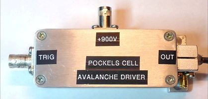
I hunted around in my pcb off-cuts box and found a piece 28mm wide x 46mm long which was just big enough for the circuit and just small enough to fit in a Pomona BNC metal box.
I scored a 15mm wide strip along the length in the middle of the pcb and with the heat of a soldering iron, removed the 15mm strip of copper from the top surface of the board to provide the isolation between the +900V supply voltage and its return, 0V, and then stuck the kapton tape over it.
Next I positioned the components on the tape, but soon realised ordinary solder would not sink into the tiny gaps between the SMD parts and I would need to add flux to them first. Looking on eBay I found three types in general offered: thick grease-like from a syringe, liquid flux no-clean, and rosin [E22]
mildly activated flux. I found an app note [E23], Pillarhouse AN301 Choosing a Flux, which recommended rosin as the easiest type to use, and purchased a small amount. The kapton adhesive became tacky with hand soldering, but held up sufficiently to complete the job and afterwards I cleared off unused flux with pcb cleaner.
Below left, the circuit from my logbook Below, heating removes copper


Left, an inexpensive pcb holder made life much easier.
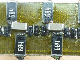
Below, after adding liquid flux and tinning the SOT23 leads individually, I soldered 28AWG wire wrap wire to all of the SOT23 legs and the rest of the components that were too far apart to solder together:

Left, the planned layout Above, freshly soldered
The PCB is 46mm x 28mm, copper has been removed below the tape
Big resistors are 2512 2W 500V peak, capacitors are 1808 220pf rated 3kV
Transistors are SOT-23 MMBT5551 selected for Vbreakdown >380V
Below, parts stuck on kapton tape Below, soldered & cleaned


Once built, the next thing was to see if it worked.
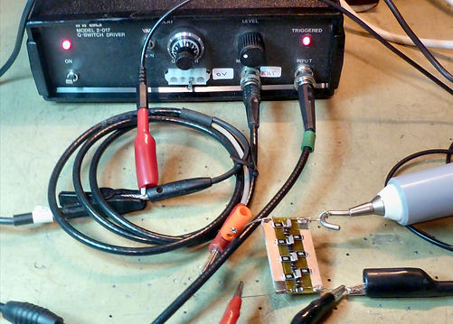
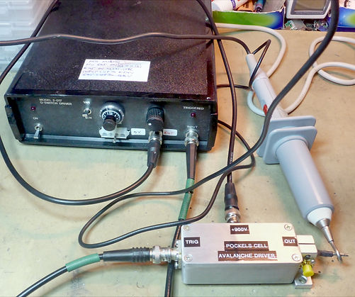
I am using a modified (see Repairs section) Inrad 2-017 Q-switch driver to generate the +900V signal for the board. Note - the 2-017 does not actually contain a pockels driver, instead it is just the power supply for one.
A Wavetek 154 [I40] provides a +6.6V 0.5Hz 1:1 pulse train to the 2-017 TRIGGER input. 270ms after the rising edge, the 2-017 produces a +900V output pulse on its MONITOR output. The rising edge of the Wavetek also triggers a Lyons PG73N pulse generator [I30], which generates a +5V rising edge 400ms after the Wavetek. this second pulse is in the middle of the +900V pulse from the 2-017,and is the trigger to the board.
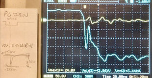
Below left, the setup Below right, the Wavetek & PG73N pulses


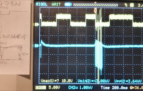
INITIAL OBSERVATIONS
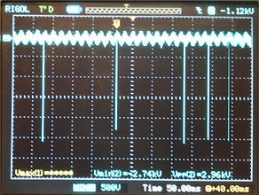
The pcb worked first time, although not off the PG73N trigger. Instead noise triggered it, but it proved the concept. I wondered if the noise was because I swapped the board trigger input resistors as I drove it from +5V instead of +10V in the cavity dumper paper. The board was also unshielded and loose on my lab bench with long wires radiating noise around it. Note - the Rigol displayed values for voltage and time become less accurate when not filling the entire screen. The indicated -3.24kV pulse is actually around -3k6V. The waveforms below are the best I recorded, but they triggered almost randomly from noise spikes, interspersed with big bursts of pulses that shouldn't be there at all.
Below left: Below centre: Below right:
The -3kV pulse wrt the Wavetek Rigol zoomed in on pulse: The fall time is fast


Having proved it worked, the next step was to place it in a shielded box as planned, hoping the spurious bursts would then disappear. I decided to use a larger, Chinese aluminium 'stomp' box instead of the Pomona. To get the pcb at the correct height for the connector pins I rested the pcb on 3 long heatshrink-covered M3 screws in the box (left), then wired in the connectors (right).

When I tested it the signals were a little cleaner but there were still multiple bursts where I expected only one negative pulse.
The EHT was also feeding back to the PG73N and corrupting its output signal, although once removed it returned to its normal state.
I added a 6.8V transzorb across the input.
One might say putting it in a nicely labelled box was premature, but shielding simplifies testing by isolating external influences.

SELF-AVALANCHING?
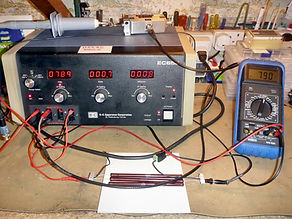
Closer inspection of all of the signals revealed the driver still fired even without the trigger signal present, indicative of self-avalanching. To prove this, I hooked up an EC Apparatus EC-650 electrophoresis PSU, which is capable of producing up to 6kV dc at 100mA. A quirk of a lot of electrophoresis PSUs is they often have complex safety circuity that inhibits the output voltage unless a load is present, that load normally being the conductive gel used in DNA sequencing. I found I could get around this by adding a 1MΩ resistor across the outputs, and below you will see the EC-650 and 3 x eBay China 40kv 3M3Ω 12W resistors in parallel for this purpose. I was able to determine my driver self-avalanched above +790V, and the higher the voltage, the more intense the self-avalanching. I didn't take it up to +900V in case it blew the transistors (the 2-017 +900V test was a short pulse, not dc):
Below, incidences of self-avalanching based on dc voltage applied to driver:
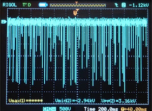
+790V: rarely (50ms/div) +800V: regularly (50ms/div) +813V: hugely (N.B.200ms/div)


The next step was to reduce the voltage to the point where self-avalanching stopped altogether, and confirm I could trigger an avalanche as intended.
OUR forum thread suggests 300Ω is gel load, not the 1M I'm using, but that would need an unrealistic 3k3W power resistor even at just 1kV ([Q1] Ohms Law P = IV = V²/R):
http://www.overunityresearch.com/index.php?topic=379.25
Outlook: \0 0 0 Overunityresearch (EC650)
Page 12 of [I37] service manual for E.C.Apparatus EC250-90 suggests 470kΩ is ok: 34W @ 4kV.
This excellent video teardown of a EC600-90 says up to 3MΩ works (I could only get up to 1MΩ to work), but then goes on to show how to permanently defeat the interlock circuitry. It's also quite a useful introduction to the safety lockout features built into most electrophoresis PSUs, for which the author finds workarounds, although I would keep the mains earth lead and use an isolated oscilloscope:
https://www.youtube.com/watch?v=4bAD37j0QGs
My EC-650 has become intermittent and awaits inspection and repair (difficult without a schematic), but when I do this I'll see if I can modify it to stop the interlock in a way similar to the above video.
REMEDIES
First plan is to add a localised bulk de-coupler, say 10µF, across the 900V supply. At this stage I don't know how much current will flow. 10µF will provide ~4.5J [Q6] which I think is a good start.
If that makes no difference, I could try increasing the number of transistors per stage from 3 to 4.
[A3], Increasing the Stability of Series Avalanche Transistor Circuits, may also be relevant.
I was still scratching my head about the worrying effect the driver had on the PG73N output. By chance I was browsing Wikipedia's: http://en.wikipedia.org/wiki/Pockels_effect [N3] and came across the following description: 'The transistors are floating and need DC isolation for their gates. To do this, the gate signal is connected via optical fiber and the gates are driven by a large transformer. In this case, careful compensation for feedback is needed to prevent oscillation'.
The later [A10] 1993 paper seems to be a transformer based design. The 1990 Cavity Dumper paper [A6] says they replaced the input transformer, but they didn't say why it was there in the first place. Their design is based on their own reference paper 3: Christiansen, K. Frank, and W. Hartmann, Nuclear Instrumentation Methods, A 256, 529 (1987), but it does not seem freely available to download.
I suspect [A10] is a copy of this 1987 design.
If increasing the transistors per stage still corrupts the PG73N output, I may experiment with a transformer or optical input stage.
Then I found a paper that went into great detail explaining the inner workings of a transistor avalanche train: [A21], Compact Subnanosecond Pulse Generator Using Avalanche Transistors for Cell Electroper turbation Studies: 'If some transistors have higher dc collector to emitter bias than others, they turn on due to dc over-voltage and the circuit produces pulses spuriously before an external trigger signal is supplied.'
Could this be the reason why my circuit self avalanched?
Even better, this paper contained a design for a high speed high voltage divider.
The next step is to try the HP8082A instead of the PG73N and see how varying the rise time affects stability, as described in the Cavity Dumper paper.
Another big difference is my circuit load is the D-dot which is only 3pF compared to the author's 11pF pockels cell. However I'll experiment with a bigger load capacitance before I risk a Pockels cell.
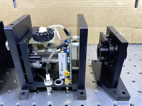
In the middle of all of this in 2018, I came across an eBay USA auction for a 'Pockels Cell Q-switch plus Polarizer for High Energy Pulsed 1064nm YAG Laser 8mm' consisting of 'a Fastpulse Technology model 1059FV-106 Pockels Cell and matching adjustable polarizer' taken from a 'Lumonics HY1200 high energy 1.2J pulsed YAG'. The most interesting part is the pockels assembly, which contains two identical naked ceramic substrates with a string of SMD transistors on them. I instantly recognised these as avalanche drivers. The strings are wired to each end of the pockels cell. Page 15 of FastPulse application note [N18]: FastPulse User Guide to Pockels Cell Drivers etc., [abbreviated], explains:
'A way to obtain fast optical switching is through the use of differential HV switches which apply separate voltage pulses to first one and then the other crystal electrode. The pulse leading edge on one side forms the leading edge (Tr) of the output pulse and the leading edge of the other side forms the trailing edge (Tf) of the output pulse. Each pulse can have a fast rise time thereby generating fast rise and fall time optical pulses in the range of 1ns to 3ns, depending mainly on the switching elements. Pulse width is controlled by the temporal spacing between the rise times of the two signals. In a differential configuration the modulator must be used in a capacitive mode. In this type of circuit, rise and fall times are sensitive to total capacitive loading and lead inductance. Therefore, wires or cables connecting to the Pockels cell must be kept very short. In fact, optimum performance is obtained by limiting the cables or connecting wires to lengths of less than one inch.'
This is why the substrates are located within the pockels cell assembly. Bearing this in mind, at first it seemed odd each SMD transistor is wired to a connector pin and socket as this must increase C & L, but I imagine these connections are essential to qualify each stage at final test.
In 2018 it was priced at $377 but in 2019 that dropped to $277, which even with shipping and import to the UK added, is a reasonable price for a modern pockels cell with twin matching avalanche drivers and a matching polariser (11 SMD transistors in the string suggested 400V each = 4400V). I bought it, partly to examine the avalanche substrate circuitry, but also potentially to use for my DIY Nd:YAG. Given the slow rate of LIBS laser pulses, I also wondered if I could use them in single ended mode, one to drive the YAG pockels and the other to drive a ruby pockels, although I didn't yet have one.
Below, double take - the white vertical object is the avalanche driver substrate, one on each side:

Q-SWITCH ALIGNMENT
The following short App note [212p02] from Leysop (UK) describes using a HeNe laser to align one of their pockels cell Q-switches: http://www.leysop.com/app_note_1_pg3.htm