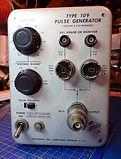
6. Tek Type 109 250ps Rise time Pulse Generator repair and 1-shot & LF modification (2020,2021)
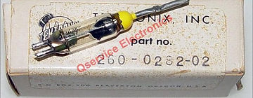
The Tek 109 pulse generator continually oscillates at 640Hz nominal, using a bounce-free mercury (Hg) reed relay to switch coaxial charge lines that produce output pulses up to +50V or -50V (±300V with an external supply) having a nominal rise time of 250ps. Due to this configuration the lifetime of the relay (Tek part no. 260-0282-0), which is now obsolete and hard to find, is reduced to ~200 hours.
https://w140.com/tekwiki/wiki/109
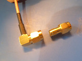
I found a working Tek 109 pulse generator for €50 on eBay France and bought it, along with a couple of spare Hg relays and two GR874 charging coax lines. I had already bought GR-874 to BNC adaptors.
REPAIR
When it arrived the 109 no longer worked, so I set about determining the cause.


109 OPERATION
The 109 produces a fixed 640Hz (nominal) output from two charge lines switched by a 360Hz oscillator. Mine can be adjusted down to about 505Hz using pot R614 intended solely for calibration to 640Hz.
Examining the 109's manual [I39] and schematic (above), the 640Hz oscillator is formed by a pair of cross-coupled PNP transistors that directly drive an electro-magnetic transformer near the relay, effectively forming a feedback astable multivibrator whose frequency is limited by the saturation flux of the transformer and the voltage applied to the circuit. The reed relay is biased by the flux of a simple horseshoe magnet; the transformer flux adds to this bias causing the reed to switch its pole between changeover contacts. The voltage is derived from a 10V zener-based regulator with a transistor drive output passing '+8V' from a poorly regulated +17Vdc supply (ripple is quoted at 1.5V pk-pk).
Note - although it's identified as signal +8V, it can be set between 7V and 10V according to the frequency adjust pot R614. For this reason I've put '+8V' in inverted commas.
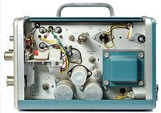
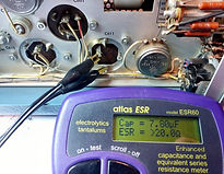
One of the first things I check on old equipment is electrolytic capacitors as they can often dry out. I checked the ESR of the two 2000µF low voltage supply reservoir capacitors C610 (good: 2960µF, 60mΩ) and C611 (bad: 7.8µF, >20Ω). Given their age, I replaced both with 105°C 25V 2200µF 20mΩ electrolytics.
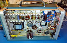
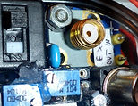
Bottom left - inside RHS. C610 & C611 are the two large cans at the bottom.


TRACING THE FAULT
Unfortunately it still didn't work. The oscillator frequency is determined by the voltage on signal '8V'. Conveniently, inside the 109 this signal is the bare wire on the nearest end viewed from the front, of the ceramic component carrier housed in the left side. On the top joint is a WE/OE wire [T16] that leads through a rubber grommet between drive transistors Q725 & Q735, into the instrument right side, where it is connected to Q627 emitter and Q725 collector.
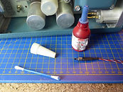
Something to note about these ceramic carriers is they are sensitive to heat and require a special silver content solder. There is actually a note to this effect on the metalwork inside, and on page 5-2 of the manual. Tek used to supply a small reel of it in some of their instruments for future repairs. By chance I had already bought 3m of a similar '96SC105' 95.5% tin + 3.5% silver 0.46mm dia solder for this exact purpose (eBay UK, £3).
This 109 had been repaired at some time in the past and some carrier joints were poor, maybe they used ordinary solder? I reworked them with the silver solder just in case.
I probed '+8V' on the carrier and found even though there was no output, the oscillator was working.


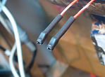
Below left - I began to suspect the magnet might have shifted in transit so I loosened and moved the red horseshoe magnet. A pulse came out, but it didn't have the expected fast risetime.
Suspecting the worst, I reluctantly decided to replace the Hg switch, right.
REPLACING THE HG SWITCH
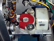
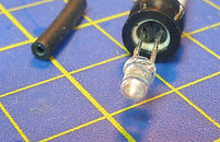
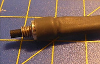
The magnetic switch assembly has a biasing red horseshoe magnet on the left, and a white electro-magnet on the right.
The Hg switch is located within the vertical metal tube behind the front panel below the assembly, its pole contact mating with the GR-874 output connector, where it is held in place by a grub screw.
Two small carbon film resistors first have to be unsoldered from the small pcb to which the Hg switch is also soldered. The grub screw is loosened using a 0.05" Allen key.


I fitted the new Hg switch and re-assembled it but it still didn't work. Frustrated, I unscrewed the electromagnet to examine it more closely.
When I refitted the Solenoid, the output appeared. It was simply a loose screw.
Photos below from left to right:
1. Wiggling the magnet produced a short pulse in some positions
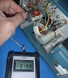
2. The 109 frequency is adjusted by variable resistor R614, visible to the right.
3. A 4mm spanner fits around a T10 bit.
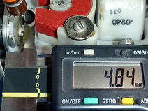
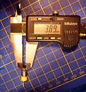
4. Some people have suggested the horseshoe magnet might lose its strength over time, so I measured it.
5. I also noted the magnet's best working position.


Below left, GR-874 charging cables need to be attached to the 109 for it to produce meaningful pulses;
a very short spike appears with no cable present. I verified correct operation using a Tek 7104 + 7A29.


1-SHOT & LF MODIFICATION
I use the 109 as a fast rise time timing reference because the Tek S-52 ~25ps TDR plugin only produces an output up to ~200mV. I don't need it to run continuously, and I wanted to preserve the Hg relay.
The modification described below adds push-button or external trigger 1-shot capability, or oscillator reduction to ~1Hz, or ~43Hz via a dedicated push-button. An internal slide switch restores the original 640Hz oscillator frequency. A high brightness LED indicates the positive portion of the pulse.
The 43Hz push button feature produces a stable two trace display on a Tek 7104 which is particularly useful for photographing picosecond rise time traces whilst minimising the display time of its MCP image intensifier, extending its life.
IT NEEDS A 1.5A PULSE
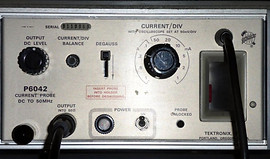
To avoid re-soldering the ceramic carrier, I cut the '+8V' wire in the middle of its carrier, fed it into a screw block and from that, extended it in a loop for the Tek P6042 current probe. The wire from the '+8V' carrier top joint leads into Q725, Q735 emitters and I found a 1.5A pulse on each cycle. With Rigol 20µs timebase, 50mV/div corresponds to 200mA/div on the P6042A. Below, photo 50615 Ch2 BE [T16] current shows 384mV pk-pk /50 x 0.2 = 1536mA, although it varied slightly. NB on slower timebase settings, e.g. photo 50616: 500µs, the Rigol displays peaks inaccurately due to lack of LCD resolution.
Below, left to right:
1 50613 Tek P6042 current clamp on 109 Hg switch '+8V' breakout wire loop
2 50614 Rigol 50mV/div corresponds to Tek P6042 200mA/Div
3 50615 Closeup view of the current pulse on the Rigol at 200mA/div
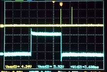
4 50616 505Hz pulses: ~1 to 1.5ms delay between BE current pulse (500mA/div) & YW 109 o/p pulse


OSC POWER UP
It seemed all I had to do was pulse the '+8V' signal long enough for the oscillator to start up and produce a single pulse, although I imagined it might take more than one pulse for the electro-magnet feedback loop to operate correctly.

I checked what happened when the 109 was switched on. The oscillator started surprisingly quickly
[my ref: LIBS 5 P.75] and with the 109 output controls set to +3.5V, after ~30ms the first pulse was ~1.7V, slowly rising over ~84ms to 3.5V.
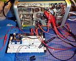
Left - closeup view of 109 o/p pulses at power-on
Right - equipment setup for oscillator startup test
HOW TO IMPLEMENT A 1-SHOT?
My first thought was to use a PIC µC as I could use a biased switch on an ADC input to select additional features such as an external input, or a slow 1Hz fixed oscillator, or to restore the 109 to its original configuration. but I thought that would be overly complex as it would necessitate adding a +5V regulator and I would probably have to add heatsinks to any output pass transistors, even if I used FETs, which would also need additional driving circuitry and then of course I'd have to code it.
Instead, I opted to base my circuit on the ubiquitous 555 timer [E50] as it can run off a supply up to +16V, can be configured both as a monostable (single pulse aka '1-shot') as well as an astable (oscillator) using just a capacitor and 1 or 2 resistors, and it can drive up to ±200mA.
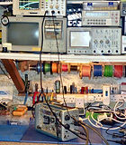
PROTOTYPE BREADBOARD
I quickly built a pushbutton-triggered 555 monostable on a breadboard using subminiature multiturn trimpots for the resistors. I added an old 3mm 10 Candela white LED (VF typ 3.5V) which was the brightest I had, driving it from the 555 Q via 180Ω current limiting resistor R5 (6.6V-3.5VF)/17mA. Bright old LEDs usually had a very narrow angle to concentrate the light, and this is no exception but it easily shows a single 3.36ms wide pulse.
FIRST PROBLEM
A 555 1-shot isn't the same as a logic 1-shot. The first hurdle was discovering the default 555 monostable circuit is re-triggerable, not mentioned in the datasheet. This means its output cannot be shorter than its trigger input. I found this particularly irksome, as normally when designing digital logic, a one-shot e.g. 74121 is by default non-triggerable and a re-triggerable one-shot such as the 74122 is explicitly described as such. Not only did the 555 output stay on as long as I pressed my pushbutton, understandably it also re-triggered from the button switch bounce when I released it.
The first step was to add a simple integrator (R3 pullup with C1 to 0V) to de-bounce the push button to 0V, followed by a differentiator (C2 followed by R4 to +V) to produce a short negative pulse to trigger the 555, with 1N4148 diodes D3, D4 to discharge the integrator and limit differentiator overshoots.
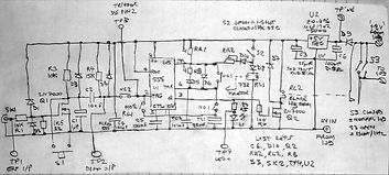
Note - see final circuit at the end for my component references.
ANOTHER HG RELAY!
I decided I could simplify the output by adding my own Hg-wetted relay which by its nature has no contact switch bounce, and I would only need to drive its coil with a relatively low current using a small logic level NMOSFET like the 2N7000.
I had already bought some 1000V 2A (3A dc) SPST Clare CUPP001A505 5V-coil Hg wetted relays to experiment with making my own high voltage pulse generator, but was unable to get a better rise time than a few µs. The Clare datasheet says it can operate up to 11V, which is greater than the 10.5V I measured as the maximum voltage I could adjust '+8V' to using R614.
Ordinarily I would drive a relay with its opposing lead to a positive supply, as positive output drivers often have a hefty voltage drop and the 555 is no different, but the 555 only has a Q positive pulse output, necessitating adding an inverting transistor or FET.
At the minimum 109 oscillator voltage setting there was about 7.3V on the '+8V' signal. I fed this through a 1N5820 (0.212VF, 20V 3A) schottky diode (D9) so I could add a 100µF bulk de-coupler (C6), further reducing its ripple, after which the voltage was around +6.6V. The 555 datasheet says its Q output drops by 0.75V running off 15V with a 50mA load, and a massive 2.5V with a 100mA load. With 20mA for a planned LED and 56mA for the Clare this comes to 76mA and I reckoned there would be a sizable drop of the 6.6V output, but the Clare should easily be driven directly by the Q output.
I drove the Clare relay coil from the 555 Q output. The Clare's datasheet mentions Zener voltage, hinting it has a back-coupled diode and zener (the best solution for back-EMF protection), but there was no explicit statement it was fitted, so I added freewheeling diode D7 and a 100Ω resistor to limit current transients into the relay coil.
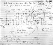
Initial 555 1-shot circuit from my logbook: Initial 555 1-shot breadboard:


BREADBOARD HOOKED UP
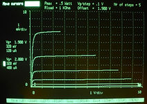
A mercury relay has to be orientated vertically so its Hg sits at the bottom and only its vapour wets the contacts. ADD NEW PHOTO 50621 OF Tek 571 CURVE FOR 1N5820
I added the Clare relay to a small breadboard that I could sit upright and inserted the Clare into the 109 driver circuit via the '+8V' signal on the top connection of the ceramic carrier:


Using the Tek P4062 I measured a 1A pk 1-shot current pulse on the '+8V' signal:


Above left, Rigol setup: although heavily attenuated due to the 100MHz bandwidth and 3.5ns [I14] scope
rise time, the Rigol trigger is surprisingly good at capturing a single 10ns wide pulse.
Above right, Rigol & P6042 setup: measuring the current pulses on the '+8V' signal passed by the Clare relay.
NEARLY A 1-SHOT
As I suspected, I could not get the 109 to produce a single pulse every time - either it missed the odd one, or else it produced 2 or 3 pulses. With 3 pulses relay life is still significantly increased. I found a 3.68ms pulse gave 2 pulses, and a 3.36ms wide pulse got 1 pulse out of the 109 most of the time, which was good enough for me.
Left, Rigol 1ms/div, YW 555 Q 3.36ms is ideal
Right, Rigol 1ms/div, BE '+8V' 555 Q 3.60ms, YW 2 pulses

EXTERNAL TRIGGER
It was tedious having to repeatedly push the button, especially as it missed so many pulses, so next I added a means of overriding the button with an external pulse generator. I wired a 2N7000 NMOSFET Q1 across the pushbutton, biased by 1M5Ω pulldown R5, protected by a 10kΩ input resistor R1 and a couple of 1N4148 diodes to the rails D1,D2, but this stopped the circuit working.
After a bit of head scratching I found unlike the milli-Ohms resistance of the push button, the 7Ω typical on-resistance of the 2N7000 wasn't able to discharge the 1µF integrator C1 sharply enough for the following 1nF differentiator C2 to produce a deep enough negative pulse. Increasing it to 10nF solved this and I was now able to externally drive the 109.
I verified the minimum external voltage needed to trigger the 109 was a CMOS-compatible 2.87V
(VOHmin = +3.5V for HCMOS logic running off +5V supply).
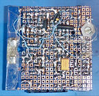
THE PCB
Satisfied, I built the circuit on pcb cut from a prototyping square pad double Euroboard and checked it worked in the 109. I added an SMA connector to the pcb for the external input.
Below left, my logbook notes showing component circuit function, and 571 curves for the 2N7000.
Below right, the pcb being cut, and first installation in the 109.


Above right, I located the new pcb to the right hand end of the ceramic carrier, beside the '+8V' supply wire to the Hg switch driver transistors, routing the '+8V' signal through a screw terminal block soldered onto the pcb. This had the added advantage of using the wire to support the pcb above the two TO-3 transistor cases below it, in addition to two nylon pcb spacers I added below the pcb.
Later I also added a thin sheet of transparent plastic below the pcb to avoid any chance of a short with the metalwork below it.
ADDING THE 1-SHOT PUSH SWITCH & LED
I needed to add a push switch to the 109 but I didn't want to ruin the 109 front panel. I noticed the top right screw holding the front decal panel in place was missing. I found a tiny APEM 9533CD + U572 button, M4 mount 30Vdc 100mA push switch in my parts box. I drilled and re-tapped the 109 screw hole as an M4, the switch now replacing the missing imperial screw. Once in, I drilled a matching hole on the opposite top left side for the 3mm white LED, which I strengthened with heatshrink.


Top CW from left, LED made and fitted front top left of 109


Above, Soldercon sockets added to LED & switch leads
Below from left, pushbutton made and threadlock added for fitting to case front top right


ADDING THE 1HZ OSCILLATOR FEATURE
I was happy enough, but for extended tests it would be useful to have the 109 able to run as a 1Hz oscillator by itself, so I added the recommended circuit to the breadboard to re-configure the 555 as an astable oscillator, an exercise I thought would be trivial - add just one more resistor between 555
pins 6 & 7 - which proved to be anything but, and instead turned the air blue over several days.
555 OSCILLATOR CIRCUIT
All I wanted was to effectively add a repeating 1 second delay to the monostable. The 555 timer monostable works by charging a capacitor TC ('Timing Capacitor') on its threshold detect pin 6 tied to its discharge pin 7, via resistor RA connected to its supply voltage. Once the charge meets the 555 threshold set by an internal string of 3 x 5kΩ resistors (where it gets its 555 name from [E50]), pin 7 discharges the capacitor.
In the oscillator configuration the 555 Q output pin 3 is fed round to the trigger input pin 2 to retrigger the monostable, and resistor RB is added between pin 6 and 7 so the capacitor C1 now discharges through new resistor RB into pin 7. However because this resistor RB is in line with the original resistor RA to the supply, capacitor C1 is charged through both of these resistors RA + RB in series, increasing the pulse width. The new discharge resistor RB produces the 1 second delay, but the charging time of 3.36ms was now increased by resistor RB, so the charging resistor RA had to be reduced to get the oscillator pulse width back down to 3.36ms. The easiest way was to switch in another resistor RA2 in parallel with RA, which I will now call RA1.
TWO CHARGING RESISTORS!
Now I had to switch in TWO resistors: RA1, RA2, each a multiturn trimpot. Given I had already built the pcb, I had limited space to accommodate this extra circuitry. I didn't want to run long wires to a switch that I had decided to install on the rear panel. Instead the easiest way of doing this was to add another relay. Around about this time I unsoldered most components and added individual sockets for them.
ANOTHER RELAY!
The smallest I had was a TO-5 DPCO Teledyne 732D-5 with a 5V coil and contacts rated 28V 1A (the D means it has an EMF suppression diode fitted). This has been in my parts box for over 30 years and these days they cost more than I paid for the entire 109! However unlike the Clare, the Teledyne can't handle more than 7V on its coil.
Right top: monostable (1-shot) circuit; right bottom: astable (oscillator) circuit.

DATASHEETS TOE A FINE LINE TO TRUTH
National Semiconductor's 555 timer datasheet boldly declares 'the frequency is independent of the supply voltage' but Diode Inc's datasheet is more truthful 'The threshold levels and charge rates are both directly proportional to the supply voltage. The timing interval is, therefore, independent of the supply voltage so long as the supply voltage is constant during the time interval.' In other words, If you have a fluctuating supply the timing WILL be affected, the opposite of NS's statement.
A 5V REGULATOR FOR ONE 5V RELAY...
To solve both of these issues I decided to fit a stable +5V regulator to power the 555 and both relays. The 555 timer takes 15mA. I checked the relay coil resistances: Clare ≥94Ω vs Teledyne ≥80Ω, both at +5.25V Vout max = 56mA + 66mA = 122mA.
A TO-92 78L05 +5V regulator only gives out 100mA so I needed something bigger, but I didn't have room for a TO-220 7805. Instead I found a TO-92 Microchip MCP1702-005 rated at 250mA with a Vin max of 13.2V. Better still, it's available in a ±0.4% version, which I bought.
You do need to read the small print however - the input capacitor ESR must be ≤10Ω and the output capacitor ≤2Ω but nowadays both are relatively easy to achieve. For the input I used a 100µF 25V electrolytic measuring 500mΩ, and fitted a 22µF 160mΩ SMD tantalum to the output on the back of the pcb.
...MAY NOT WORK WITH EVERY 5V RELAY
With the +5V regulator added the Clare output relay no longer worked and the benefit of direct drive from the 555 had gone out of the window: the 555 timer's output voltage had dropped, and was now unable to guarantee the Clare's 3.5V minimum pull-in voltage would always be met, revealed when I tried the circuit; I had forgotten what I had read earlier in its datasheet.
I was now forced to buffer the 555 Q output, throwing away the final advantage of using a 555 over a PIC.
Right, a pcb jig is very useful for debug:

ANOTHER FET!
Faced with the task of beginning all over again or continuing with the overcrowded pcb I decided to soldier (solder..?) on and the last step was to add another 2N7000 NMOSFET Q2, correspondingly inverting the Clare relay driver topology.
Left, revised circuit with 2nd FET Q2 added
Right, revised layout with 2nd FET Q2 added

SHORT PULSE ON A LONG DELAY = TROUBLE
The Teledyne relay now gave me the ability to select 1-shot or oscillator mode but no matter what I tried, I could not get the astable and monostable pulse widths the same; I could get either but not both, maybe because the ratio between 3.36ms and 1 second is 336:1 so the R/C combos needed were at opposite ends. Even by adding diodes between pins 6, 7 to isolate the charge and discharge paths, I
still could not get them equal, possibly due to diode reverse leakage current with the high R value.
With a monostable 3.36ms pulse the closest I could adjust the astable pot to was 2.48ms but this was due to the range of adjustment of the pots reduced at opposing ends of the extreme ratio: one around 29kΩ, the other around 85Ω, with my nearest available pots being a 100kΩ & 2k2Ω respectively. Ideally I would have added a series R to each but there wasn't space on the pcb. Seeking alternative circuits to reduce component count, I also built circuits on the breadboard utilising 555 control pin 5 (recommended for PWM control) and 555 reset pin 4 (to actively control the pulse width), both to no avail.
I found the pots had sufficient range of adjustment for the monostable with C1 = 100nF but the astable worked best with C1 = 22µF. Eventually I ended up with 3 multiturn trimpots and two capacitors. It didn't help that due to space restriction the trimpots were not all facing the same direction and I couldn't see their values as I adjusted them, repeatedly forgetting some were CW and some CCW, but I did eventually get there. In the circuit I've renamed these components RA1, RA2, TC1, TC2, where T = Timing.
The procedure for setting RA is to first set the 1-shot pulse width using RA1 then adjust RA2 to set the 1Hz osc pulse width.
Even though charge and discharge paths are separated using diodes, I suspect reverse leakage current means there is still some effect so next check osc period and adjust RB if necessary, then fine-tune RA1 & RA2 too.

ADDING THE NEW TOGGLE SWITCH & BNC TO REAR OF 109
I decided to feed the external trigger in through a BNC at the rear of the 109 and bought a pre-made chassis mount BNC to SMA lead from eBay China for a few $. Unfortunately the only SMA/BNC cable I could find had a socket in the SMA, the same sex as the pcb SMA, so I also bought an SMA male to male adaptor. This increased the height of the cable off the board making it a very tight fit to get the side cover back on the 109; functional, but less than ideal:


I was apprehensive about drilling two holes in the back of the 109 box because I assumed the puckered Tek blue outer metal cover was steel. I thought about separating it from the inner chassis but it was too fiddly to unsolder the fuse which I had already covered in (yellow) heat-shrink to avoid touching the lethal bare mains wires whilst I worked on it, although I was using an RCD. My fears evaporated when I discovered the entire metalwork is soft aluminium and I drilled the holes with ease. For reference, the centre of the fuse holder seems to be around 24mm from the edge of the case (being American with imperial measurements I was expecting exactly 1", but perhaps this was just a loose tolerance). I aligned my own hole centres and added the switch and BNC, its inner flange just missing the stepped inner support frame for the central mounting chassis in the 109:


Above right - I had already covered the exposed mains wiring on the fuse holder at the back of the box with yellow heat-shrink but I was increasingly concerned about working with exposed high voltages on the transformer, so I added a plastic safety shield over it, secured by PC motherboard supports inserted into rigid plastic tubes on the ends of the transformer mounting screws.
43Hz FEATURE
Whilst testing the 109 I found my Tek 7104 + 7A29 could easily display a single 109 pulse, but not a second channel from the Pearson 410 current transformer I was pulsing in an experiment, solely because of the low repetition rate - when I ran the 109 at its normal speed both traces appeared together.
At 1Hz or slower, one or the other appeared, but not both, despite the delay between them being in the order of nanoseconds. To ensure the two signals were temporally aligned, I used separate 7B10 timebases.
I needed to run the 109 faster than 1Hz to get both channels to trigger, but the external trigger only works up to ~15Hz because it feeds into the capacitively filtered push switch 1-shot input. I concluded the best idea would be to add another momentary push switch to override the 1Hz signal with the faster frequency. As with the front panel, I tapped one of the top Tek rear panel retaining screw holes and replaced it with the new push button.
I tried using the new push switch to parallel a new capacitor with TC1 to reduce the 555 frequency, but that reduced the 555 pulse width which could not be resolved without more resistor changes.
Then I remembered the whole design concept behind the 109: its oscillator frequency is dependent upon its input voltage which is derived from a buffered 10V zener, D612. The question remained whether there would be enough change in frequency over voltage of which to take advantage. I inserted a voltage source in place of the pcb and created a table of the 109 voltages vs output frequency read off the Rigol and noted the 109 oscillator frequency increasing wrt voltage.
Voltage source 109 output Below - the new 43Hz push switch:
0 to 5.30V OFF
5.40V to 5.44V 0 to 3Hz
5.45V 2 to 10Hz
5.46V 10 to 52Hz
5.47V to 5.49V 16 to 52Hz
5.50V to 5.54V 23 to 53Hz
5.55V to 5.64V 23 to 55Hz
5.65V 35 to 55Hz
5.66V to 5.74V 23 to 100Hz
5.75V 41 to 100Hz


ANOTHER ZENER!
The relatively wide 140mV band between 5.50V and 6.64V looked viable: I didn't want to run the relay faster than 55Hz as that would reduce its life, and the 7104 displayed two traces down to 23Hz, although it wasn't ideal for photography. The simplest way to reduce the voltage was to add another lower voltage zener in parallel with it, and a TL431 shunt requires the minimum of components to produce a variable output. I bought the tightest spec 0.4% TL431B and built a prototype on the breadboard to prove I could easily set the voltage within the band, then added it to the pcb. Initially I set the frequency to 55Hz but later fine-tuned it to 43Hz. This sounds an odd number, but it was the optimum tradeoff between relay frequency and flicker on the 7104.

The Q output was now producing identical 3.36ms pulses on both the monostable and the astable.
DUAL TIMEBASES = TEMPORALLY ALIGNED CHANNELS
When no coax charging cable is present, the 109 produces very short twin 1ns pulses on its output. As this is harder to trigger off than the wider pulse employing a charge line, I used this worst-case signal to select the ideal frequency for dual trace photography. I fed this 109 output into separate 7A29 plugins triggered by separate 7B10s with independent horizontal trace adjustment. Had the same 7B10 been used for both, there would be a delay between them. An alternative solution is to use a 7A29 1GHz plugin with the ±500ps delay option, but I didn't have one of those at the time. Many modern scopes don't have this feature, even if they have dual timebases.
Top right, the slight waveform mismatch may be due to 7A29s being different designs; left: digital 7A29P vs right: analogue 7A29 and no 7A29/7B10 plugins being calibrated.
Bottom right, in this photo I'm pressing the 43Hz push switch on the back of the 109:


ALMOST THERE
I was still not there. If the 109 was at room temperature and I turned it on, as it warmed up I noticed the 1Hz oscillator delay between pulses varied considerably, up to ~200ms over the first 15 minutes. This period was chosen arbitrarily and isn't critical, but I wanted to know why it changed.
109 ZENER
A freezer spray revealed Tek 10V zener D612 was the culprit. I thought about adding an external pot in place of RB but soon realised I'd be twiddling it forever. I thought of building in an auto-regulating NTC thermistor circuit into the ground lead of the regulator but feared it would take a huge effort to calibrate. Instead, without thinking I added a small (eBay China) 80486 CPU fan to cool it.
TEMPERATURE TESTS
Nothing improved. I attached K-type thermocouples (TC#) [E56] to everything I thought could get hot, feeding them into my old 8-channel RS-232 Pico TC-08 Data Logger running its somewhat rudimentary PicoLog software. Initially I included the OB2 108V valve regulator V679 and all TO-3 transistors, but they didn't get significantly hot so I didn't take screenshots:
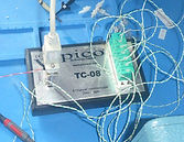


Screenshots below far right - even with TC6 attached to the back of the zener, the curves reveal its sharp voltage fluctuations directly followed the pulsating cooling air from the fan in front of it:
PicoLog thermocouple channel locations:
TC8 (left side) 109 Transformer
TC6 (left side) 109 Zener D612
TC5 (left side) Clare relay top surface (ie mod pcb)
TC1 (right side) R626 (big resistor far right)
Cold Junction Ambient reference internal to TC-08


The sharp dips at the start are due to me adjusting the masking tape holding the TCs to the Clare relay and zener; I didn't re-run this test because it was evident what was happening, and I removed the fan.
THE 109 IS ONE CRAZY HOT BEAST
I attached TC1 to the big 6Ω resistor R626 at the back of the 109 on the opposite side of the transformer, that I had ignored up until now. When I switched the 109 on, R626's temperature shot up to over 240°C. It wasn't just the transformer getting hot, it was this resistor on the other side (25W rated according to the manual), whose sole function is to crudely regulate the voltage to the Hg relay feedback stage by dropping it into power PNP Q627, buffering the zener. Initially I stuck TC1 on with masking tape and it was only when I smelt burning I realised my mistake (see brown mark on top of R6), and instead affixed TC1 with a piece of uninsulated wire. With the regulator set to its minimum voltage, it now had more volts to drop; what an awful design.
I checked the 17Vdc supply and confirmed 17.13Vdc, spot on. I measured the voltage across and current through R626 for the 109 minimum and maximum frequencies with variable resistor R614 at each of end of its travel (but no output pulses), and I ran temperature tests for both, see results below.
Fmin 1.28A to 1.80A, 10.56V across R626, 246°C: Fmax 0.90A to 1.36A, 7.85V across R626, 172°C:


Above far right, the sharp rise on the Clare was due to me re-positioning its TC5 closer to the relay.
FORESIGHT
Even though I'd turned off the oscillator, this resistor was of course continually dissipating heat. Oh for foresight: I should have realised this at the beginning. I had wrongly assumed from their size that the big TO-3 transistors in the Hg switch driver stage were the heat culprits, and being located near the high voltage OB2 valve regulator V679, I had thought the big R626 was part of its circuitry. How soon one forgets lessons learned long ago: 'Never assume anything'.
HINDSIGHT
I feel a certain affinity for researcher Dr R. Abergel working on Einsteinium at UC Berkley, describing her paper as 'a long series of unfortunate events':
https://chemistry.berkeley.edu/news/discoveries-edge-periodic-table-first-ever-measurements-einsteinium
My tests reveal it took well over an hour for R626's temperature to stabilise, unnecessarily dissipating not only in this resistor but in the transformer too, and excess heat is never good for component life.
The first step I should have undertaken before anything, was to replace the entire zener regulator: D612, R6, Q627 and support components with a tiny, cheap, cool, Nat Semi 'Simple Switcher'
LM3596S 1.25V-35V 3A step-down module from eBay China. I was initially concerned about using a switcher to drive an inductive load, but I used one of these to power the 24V 2A choke stepper motor I put on my futuristic motorcycle, see [Projects: Fish & Chips] and I'd had no problems there, so I bought it.
I'm holding off for now though, as the time between pulses really doesn't matter a lot; I only added it for convenience to save having to keep pressing the 1-shot button. If I need more stable timing I will have to replace the 109 regulator and if I do that, I won't need the TL431B.
After pulling my hair out for the best part of a month and finally achieving a 555 timer based solution, I've had enough of the 555 timer's idiosyncrasies. I still can't believe such a simple concept needed so much effort and I now bitterly regret not using a PIC because I could have used it to regulate the supply voltage AND built in a software-controlled frequency feedback control loop. I may yet build a PIC version purely out of contempt for the supposedly wonderful 555.
First I have to cool off a little myself.
FINAL LAYOUT


FINAL TEST & CIRCUIT
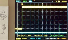
Final test of the pcb at a lab temperature of 27°C with a freshly powered 109 revealed the 555 Q pulse width had increased to ~3.6ms with the osc setting ~830ms between pulses. As there no longer seemed to be any missing pulses and it also worked on each press of the push button, I left it at that. Using the Wavetek 154 [I40] as a programmable voltage pulse generator, the minimum external trigger input
voltage= +2.9V (HP3468A), and the delay from the rising edge to the 109 output pulse = 4.57ms:


I need to repair the 7104 graticule lamps - they work, but their PSU doesn't. The lab light was off to photograph the following waveforms so instead I have enhanced each photo's gamma to show the graticule.
Although the pulse is as fast as expected, the 7104 shows a long slow curve at the top of the rising edge. I had long suspected this was due to the low quality 50Ω coax cable I used between the 109 output and the 7104, 7A29 input but when I repeated the experiment using air lines I found no improvement.
Measurements taken with long GR-874 coax charging cable on 109:


In 2023 I splashed out and bought a used Rigol MSO8104 that had been upgraded to 2GHz and discovered the 7104 itself is the culprit. To the right is a tekwiki photo of what the 7104 risetime should look like from the Tek 067-0587-02 Calibration fixture:
Tr ~240ps, assuming cal fixture 150ps then
7104 rise time = SQRT(240ps² - 150ps²) = 187ps:
https://w140.com/tekwiki/wiki/067-0587-02#/media/File:Tek7104-ristetime-1000hz.jpg
More 7104 rise time images from the author here (3/4 down page):
https://w140.com/tekwiki/wiki/User:Peter
On the MSO8k I measured 170ps average using a Brodgar pulse generator calibrated at 34ps. This means the MSO8k rise time = SQRT(170ps² - 34ps²) = 167ps.
ADD MSO8k PHOTOS

VIDEO
Setup: 109 1Hz output with long GR-874 coax charging cable:
506v01 P1340717 109 1Hz long coax Rigol & 7104.MP4 - 8027MB
109 RISE TIME
TBD
Setup:
Long GR-874 coax charging cable on 109
GR # airline between 109 & 7104 7A29.
[Q3b] Calculate true 109 output pulse rise time:
signal Tr = SQRT (measurement^2 - 350ps^2 )
True rise time = SQRT (MEAS^2 - 350ps^2) = ps.
DATASHEETS
µ Ω ± °