4. Prototype Integration
I now had a working Nd:YAG laser as well as a system that could detect up to 80 elements from atomic wavelengths in plasma, and it was time to integrate the two systems to build the LIBS system.
However all was not to go as smoothly as planned (it never does).
Whilst I had been learning how to use the PCM401, a nagging doubt had formed in my mind, that I had never solved. This was the question of the minimum period of time the sensor was exposed to plasma whilst it controlled its process. There was no explicit statement in the embedded help, but there were hints it was no faster than 100ms (online help file: 'If the integration time is set for 100 milliseconds, then a new spectrum appears on the monitor every 100 milliseconds.'. However no minimum integration limit is described. There is also an unspecified program Gate time, see below).
This is far slower than the 4µs - 100µs period in which I hoped to capture atomic spectra long gone by 100ms. This period is described in the diagram below from Kigre's datasheet for the MK367 [O6]: 10ns for laser plasma ignition, around 1-2µs for intense Bremsstrahlung ('braking') radiation where the atomic forces sorted themselves out, followed by the release of useful spectra up to 100µs and beyond.

Diagram reproduced with kind permission of Kigre, Inc.
Normally LIBS systems employ optical sensors with a gating feature that only turns them on when they are needed (the Stellarnet PortaLIBS has such a signal) and this can be down to nanoseconds, but the only mention of a gate signal in the PCM-401 help is 'The Gate width can be arbitrarily long or short, but the program cannot respond sensibly to a gate width which is shorter than the time interval between data acquisitions.'
A start would be to determine by the size of the sensor and its data transfer time, but I fully expected the code execution time would be greater, and I didn't hold out much hope given the relatively long seconds to minutes duration one might expect of a semiconductor fabrication process; there would be no point making it faster than necessary if it (very likely) cost more to do this.
A label on the black box at the rear of the Sp-275 said 'PDA Detector', so I knew its sensor was a photodiode array, most likely linear, but there was no mention of it in the embedded help, although there were warnings it had an image intensifier that could increase sensitivity up to 10,000 times, and it was important to keep it to the minimum usable setting at all times to avoid damage, which of course I heeded. I found the minimum was 2 out of 100 - if I set it to zero the spectrograph was just noise.
Another thought occurred to me - my ungated EPP2000 Stellarnet spectrometer had been able to pick up the 1064nm from the MK367 laser when triggered from its optical input, so perhaps the PCM-401 could too? However if it did this with no control over the gate, amplification through the intensifier could be certain death for it, if not the PDA as well.
I was wary of opening the PDA assembly because I didn't want to introduce dust between the intensifier and PDA, or risk misalignment, but any sensor would very likely be mounted on a PCB, and that PCB would be behind the intensifier, so it should be safe to remove the back cover and look inside - there might be a label identifying the sensor.

The PDA rear cover was held in place with hex security screws.


Opening the unit, it appeared there were at least two pcbs because no sensor chip was visible on the top pcb, immediately visible. Examining it, I found most of the logic chips were counters as expected to drive a linear PDA. Unfortunately removal of the pcb is hindered by an aluminium spar heatsink for a TIP120 transistor (NPN, 60V 5A) and a gold-coloured 4Ω 25W aluminium power resistor.
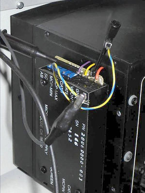
The spar is attached to the inside left wall, the same side as the external HIGH VOLTAGE warning label. Inspection of the label revealed it to be on a cover that was retained by two black hex screws on the outside and two uncoloured ones on the inside near the front left. When I removed them I could remove the cover and inspect the PSU, a 1994 GBS Micro Power Supply model 2006000-003, with all connections clearly labelled, confirming it was designed to drive an image intensifier tube. Of significant interest was the GATE signal which leads to a connector on the top pcb via a purple wire. I searched in vain for a datasheet for the PSU. All I could find was one embedded in a paper for an older 1988 type without the GATE input: [D22], but at least this gave some insight into its operation.
Purple wire top right: TIP120 & 4Ω on spar: MCP HV PSU behind left side cover:


The only way I could see to remove the top pcb to gain access to the sensor on the lower pcb would be to remove the the spar heatsink, and the only way I could see to do that would be to unsolder the top 4 connections to the PSU and unscrew it from the side of the unit. Although trivial, I was reluctant to do this on working equipment. It wasn't critical that I knew what the sensor chip was; all I wanted to know was how many elements it had, and I could find that out by analysing the signals from the PC. Of much greater interest was the GATE signal on the PSU, and I could examine that at the same time.
The potential inability to gate the sensor to a short detection time wasn't the only worry. Of much greater concern was the likelihood of the Bremsstrahlung radiation intensity, or a reflection from the laser, damaging the image intensifier which was probably a sensitive (expensive and irreplaceable)
Micro-Channel Plate (MCP).
Of further interest was the PDA itself; it now seemed there was a gating mechanism for it; perhaps if I knew the timing, or how fast it was read, I could devise my own gating control circuitry. The PCM403 auction had said it was fitted with a 1024 element PDA but that was a much later unit. It seemed more likely the PCM401 had a 512 element PDA, but I could not prove it. I wanted know how long the PCM401 took to read the PDA and I could find that out with a bit of reverse-engineering...
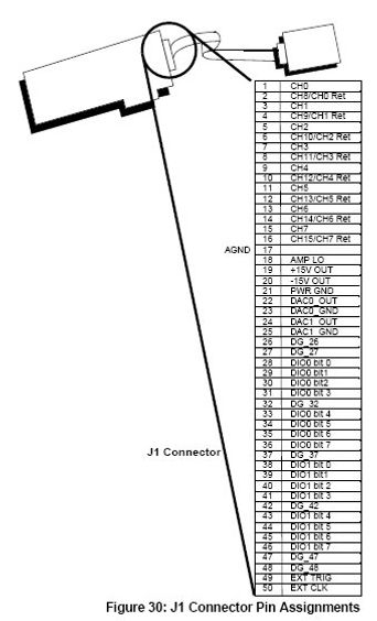
I could not examine the software as it was already installed, but I could examine the waveforms between the PCM401 PC I/O card and the Sp-275 PDA sensor. Once I realised the I/O card was a Data I/O 16-bit ISA DataAcq DT21-EZ I found a datasheet [D24], which revealed it has a selectable 16 channel 12-bit ADC and a 2-channel 12-bit DAC as well as 16 digital I/O signals:
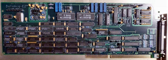
Left: The DataAcq DT21-EZ I/O card with its 50-way flat cable connector on the metal bracket to the right.
I also decided to look inside the Universal Interfacer II box that I now realised was the interface to the process equipment because it had two rows of quick-connect terminals on it labelled DIGITAL INPUTS and DIGITAL OUTPUTS. By cross referencing the I/O card pinout to the pcb and examining the circuitry whilst manipulating the I/O via the software, I was able to work out which I/O signals were assigned to the box, which I duly labelled, adding small schematics of the respective interfaces.

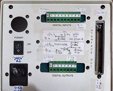
The Interfacer II box (above right photos) has a 50-way IDC plug on the front and back, and as far as I can tell is intended to go between the PC and PDA and provides the means by which the PCM401 communicates with external equipment. It occurred to me I should be able to use it to examine signals between the PCM401 PC and the PDA. Unfortunately I only have one cable, but having pulled it apart and verified it was just a standard 1:1 flat cable, I realised I might be able to use a near-identical standard flat 50-way PC SCSI cable for the second connection. I hooked it up from the Interfacer box to the PDA but the system didn't boot. I'm not really surprised - the system is designed to accommodate shielded cables and my SCSI cable isn't shielded, and the added length would not have been easy for it to drive cleanly. I did find however that the system worked if I used my SCSI cable between the PC and the PDA. This gave me another idea: I could use my SCSI cable as a signal breakout instead of the Interface box which ironically would have been harder to use for this purpose.
I added labels each side of one of the SCSI cable's many female connectors, identifying the signals from the DataAcq DT21-EZ card datasheet. The female connectors made it a breeze to stick wires in to access its signals. My Rigol DS1102CD is a now obsolete mixed mode 100MHz DSO with a 16-bit Logic Analyser built in and initially I set up its LA to examine the digital I/O, but the LA must have added too much capacitance to the lines because the software refused to run. Instead I had to use just the two analogue probes to examine each signal in turn until eventually I learned how the I/O card communicated with the PDA. A really neat feature of the Rigol is its Ultra-Zoom, which allows you to show a relatively slow signal as well as a zoomed in section of it, ideal for determining the number of clocks in an otherwise unviewable solid block.
Below left: the SCSI breakout cable between the PCM401 PC and PDA Below right: breakout signals
Below left: PDA video output for 512 elements corresponding to the resultant spectrograph of the lab's 100W tungsten ceiling light:


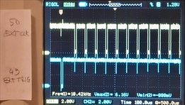
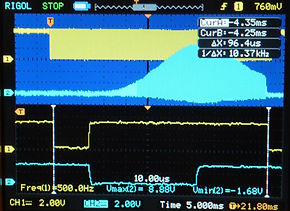

Top: 49.4ms PDA video clock burst Top: EXT TRIG starts burst
Bot: 49.4ms/96.4µs = 512 clocks Bot: 20µs to video data out
Although I could not individually count the number of clocks, the fact the burst took 49.4ms and the time between each clock was 96.4µs (courtesy of the Rigol Ultra-Zoom facility, see split view above) meant there were 49.4ms/96.4µs = 512 clocks present on signal EXT CLK, pin 50 of the I/O card. It was definitely a 512 element sensor. The PDA video appeared on I/O card ADC channel 0 on pin 1 following the rising edge of the clock on EXT CLK. The only other signal that seemed to be involved was signal EXT TRIG on pin 49, which initialised the video clock burst. This appears to be a very noisy line but my scope probes were grounded to a nearby digital ground on the cable, a long way from the source.
The sensor has 512 elements and it would have to have a quartz (or bare) window for the spectrometer to go down to 200nm. With 1995 being the year of manufacture it could be a 1MHz Reticon RL0512 [D2] or a 2MHz Hamamatsu S3901 [D21]. Based on my later research at the bottom of [Plasma Chemistry monitor], I think it is most likely the S3901 since I had found its predecessor the PCM400 used a Hamamatsu S2031 which has PD elements with 50µm spacing and 36µm aperture long x 2.5mm wide, and the Reticon RL0512 is only 26µm wide. Hamamatsu parts with 50µm spacing and 2.5mm width being a repeated feature for all of SC Technologies' PCM systems suggest the PCM401 sensor is an S3901 even though its aperture differs by being 45µm instead of 36µm. The S3901 is in Hamamatsu's April 1990 catalogue [D20] so would have been available when the PCM401 was built in 1995.
Interestingly, the PDA output burst occurs continually regardless of the whether a recording sequence is started or stopped on the PCM401.
I experimented with the software selectable integration time and found With a selected minimum integration time of 100ms each block of 512 clocks was spaced 98ms apart, extending to a maximum of 2624ms for an integration time of 2.5 seconds.
The integration time determines the distance between the blocks of pulses and with the minimum 100ms integration time, the total cycle time for each PDA bock read was 149.1ms, or roughly 150ms which means the system should be able to run at 1/150ms = 6.7Hz max. Having said that, with integration fixed at 100ms, as the video comes out at twice that rate I think it could be increased to at least 10Hz.
Later, I came across a 1997 paper on the web [O50]: 'A SC Technology Plasma Chemistry Monitor 401, consisting of a spectrograph with a gated, intensified, photodiode array of 512 elements, is used as an optical multichannel analyzer to obtain emission spectra simultaneously in the range from 200 to 1000nm with a 4nm bandwidth'.
IMAGE INTENSIFIER GATE TIMING
Having determined the signal timing for the PDA, the next step was to examine the GATE signal on the image intensifier HV PSU to see what it did. What I found was disappointing: it stayed low for the entire duration power was applied to the PDA, regardless of the state of the PCM401.
Below - probe on GATE wrt 0V Below - no GATE visible on pulses Below - no gate on clock bursts


Below: GATE only goes high when power is removed:


However during the process of making this measurement I noticed the VGA monitor colours changed from normal to a lurid purple. It didn't stop it working and when I removed the probe it went away, and I thought nothing more of it. Later when I came to use the PCM-401 again I found the image intensifier appeared to be stuck full-on and realised I had damaged it during the measurement. I had taken ESD precautions so it seemed unlikely that was the cause. It occurred to me connecting the Rigol scope probe ground clip to the GND pin on the MCP PSU could have been the culprit; given the high output voltage of the MCP PSU, what if it was a floating supply, achieved by opto-isolating its signals from the PC I/O card ground, and I had inadvertently shorted it out? As a temporary work-around I re-calibrated the PCM-401 with the fault as it still worked otherwise, but significant use would seriously degrade the intensifier and shorten its life. The fault might only be on the I/O card, but it could be the PCM I/F or worse, the MCP PSU itself. Whatever it was, it needed repair.
I couldn't find a datasheet for the PSU, but I found [D22]: GBS Micro Power Supply model 200057 Generation 2 image intensifier HV PSU datasheet, which appears to have similar connections.
It occurred to me I would need a means of determining how it worked without repeating the same mistake, which meant finding an oscilloscope with inputs that were isolated from the common ground on my Rigol. Even if it wasn't the problem, I'd feel a lot happier probing unknown circuitry this way. After a little research and a delay until an affordable one came up on eBay, I settled on a Tek THS720P 100MHz 500MS/s DSO, see [References: Oscilloscopes].
Google AI suggested the TIP120 may be part of a ground isolation circuit to enable the MCP psu ground to float above logic ground and I could potentially have shorted it out, but I fail to see why this would need to be an active circuit. That said, I have nothing to lose by checking if it still works.
I NEED TO CHECK IF THE I/O CARD DAC O/Ps STILL WORK - ONE OF THESE MIGHT BE THE MCP GATE - [D22] DATASHEET FOR OLDER MCP PSU HAS 0-10V CONTROL INPUT. THIS IS LIKELY THE GATE SIGNAL. ALTHOUGH I RECALL I COULD NOT FIND EVIDENCE OF AN ANALOGUE O/P AT THE TIME. COULD INSTEAD THERE BE A DAC ON THE PDA BOARD DRIVING THE MCP, AND ITS OUTPUT FED BACK TO THE PCM VIA AN ADC I/P?
PCM ACQUISITION TIME
I came across this statement on Page 173 of [L11], Plasma Processing IX, Proceedings Volume 98-4 of the ElectroChemical Society: '...Plasma Chemistry monitor PCM403 was used to capture optical emission spectra of plasma. Time for capture a single spectrum is 0.26sec.' (260ms = 3.85Hz).
This prompted me to re-examine Telemark's fall 2009 brochure offering the final version PCM420 [O10]. I found its 1024x256 CCD could only manage a 40Hz (25ms) sample rate. This was a good decade after the PCM401, and still very slow for LIBS. In fact ungated, I suspect all these systems are too slow for fast LIBS laser pulses.
Image intensifier
Hamamatsu articles on MCP image intensifiers [D14],[D15] said a high voltage gate signal is a mandatory requirement due to the way they worked.
I spotted an auction for a 'SpectraPro-275 monochromator with IRY-1024 S/RB intensified diode array detector'. The descripton said: 'The IRY-1024 S/RB is a proximity-focused MCP image intensified diode array detector. These detectors are for medium to low intensity signals, 180-900nm.'.
I Googled for 'IRY-1024 S/RB MCP' and found the 1997 Princeton Instruments catalogue [O47] with a girth of information on detectors, and on page 37, a datasheet for their RY series of PDAs. Page 71 lists the
ST-116 as a suitable controller, which is described in detail in the controller & operation manual for their ST-1xx PDAs [O48].
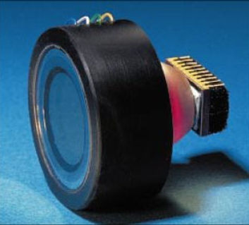
[O48] Page 64 says: 'An intensified diode array detector consists of a wide aperture (2.5mm) diode array optically interfaced to a proximity-focused microchannel plate (MCP) image intensifier through an optical-fiber coupler.'
'The combined high gain of the MCP image intensifier and the low readout noise of the diode array result in a very sensitive detector capable of responding to a single photoelectron. The MCP is composed of more than a million individual miniature electron multipliers with an excellent input to output spatial geometric accuracy. Intensifier gain is factory adjusted by varying the voltage across the MCP or the voltage between the MCP output and the phosphor. [...this second parameter affects both the gain and the resolution of the intensifier...]. The voltage across the MCP can typically be varied from 500-950V.'
The statement 'through an optical-fiber coupler', together with a picture of such an assembly (right) made me realise there was no harm looking deeper inside the PCM-401 PDA, since I could not introduce dust between the MCP and the PDA.
The PCM401 intensifer gain is adjustable so I assume SC Technology selected a part whose resolution met the needs of a 512 element PDA for any selected gain.
Even more interesting, page 74 of [O48], Gating Modes for Intensified Arrays, is the beginning of a large section that includes voltage timing diagrams for numerous applications including lasers.
[O49], Princeton Instruments Manual for the PG-10 Pulse Generator, provides even more information.
Wikipedia also provides some good background information, such as the limited lifetime of these devices:
http://en.wikipedia.org/wiki/Image_intensifier
It is possible, though unlikely (or else there would be no point in connecting a signal to the MCP PSU GATE input) there is no active gate signal because its timing might not have to change if the instrument is only used for slow plasma signals, and it would be cheaper to keep it as an internally generated, fixed signal. The whole PDA clocking sequence started on the falling edge of a 16µs wide pulse on the I/O card pre-assigned EXT TRIG signal. However some intensifiers don't have a maximum gate time and can be operated from dc. This could very likely be the case for the PCM-401.
I began to think of workarounds. If the intensifier gating time was fixed or dc, perhaps I could add a mechanical shutter to block out everything until the Bremsstrahlung radiation had ended? Better still, if I used the leading edge of the shutter to trigger the laser, there would be minimal jitter due to its motor.
At this point I had to go back and look deeper into how lasers work; normally a Nd:YAG laser emits varying pulses of light. Only by adding a special modification called a Q-switch is it be possible to control that light by forcing it to appear as a 'giant' pulse. The timing of this pulse can be controlled and thus synchronisation is possible.
The MK367 has an internal Q-switch and at first it seemed feasible I could use a mechanical shutter to block radiation from the intensifier before atomic spectra appeared, but the MK367 has a passive Q-switch, consisting of a specially treated block of glass called a saturable absorber, that blocks light passing through it until it becomes saturated and crosses a threshold of intensity, whereupon it releases the light in a single short pulse before reverting back to its original state:
https://www.rp-photonics.com/saturable_absorbers.html
Saturable absorbers suffer from poor timing repeatability as there is some hysteresis in the threshold point and recovery period between pulses [O55], MIT EE & computer science: Chapter 8 Saturable absorbers. As a result of this if I used a mechanical shutter to fire the MK367 I would not be able guarantee the shutter would be synchronised to it, and damaging radiation could get through to the intensifier.
Unless I could get the intensifier gate to work, I would need an actively Q-switched Nd:YAG laser that could be synchronised to the shutter.
That left two options:
a) find a way to extend or amplify the atomic signals so I could remove the intensifier, or
b) buy or build an actively Q-switched Nd:YAG laser, see [Q-Switches].
Next I set about achieving both of these goals.
However - it was only in 2018 I discovered there would most likely be a FO conduit glued to the PDA to route the incoming optical signal from the intensifier. If it was indeed stuck with adhesive, this might make it rather difficult to remove the intensifier from the PDA.